Look into the chip
Quartus (environoment from Intel) have a featur that show how our design looks inside the FPGA chip.
The material is available in video and text versions.
As an example, we will use the project FFT, which can be downloaded from the repository. After launching, we will see the main Quartus window (Figure 1). Start the construction of the project by clicking Compile Design (1).
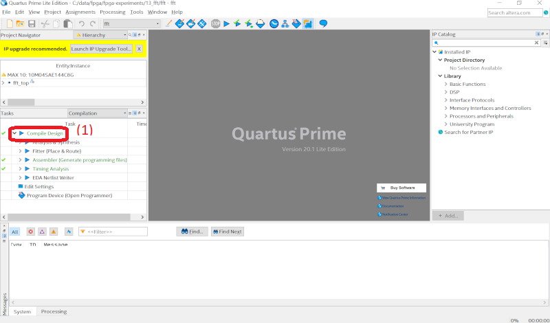
Figure 1. The main Quartus window
Then, from the Task window on the right, expand: Analysis & Synthesis (1) -> Netlist Viewer (2) and select RTL Viewer (3) as shown in Figure 2.
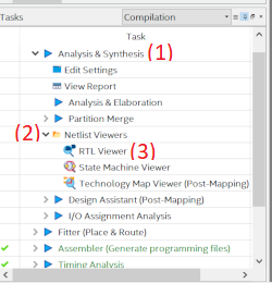
Figure 2. Task menu
A new window will open in which we will see our project drawn at RTL (Register-transfer level). It is a high-level way of showing logic. It is not related to the structure of the FPGA (Figure 3).
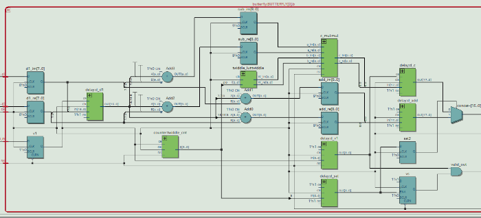
Figure 3. RTL viewer
Then we will go to the next view: Technology Map Viewer (Post Fitting). It is presented in Figure 4.
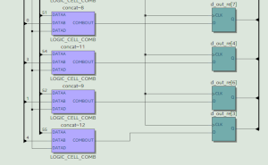
Figure 4. Technology Map Viewer (Post Fitting)
Here we only see the components that are available in the FPGA chip. We have a second, Technology Map Viewer (Post-Mapping). It is similar, but this time individual blocks are assigned to specific places in the structure of the system. However, we will move on to the next view. In the Task tab, expand Fitter and select Chip Planner (Figure 5).
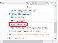
Figure 5. Task menu
When we select it, we will see a window similar to the one in Figure 6.
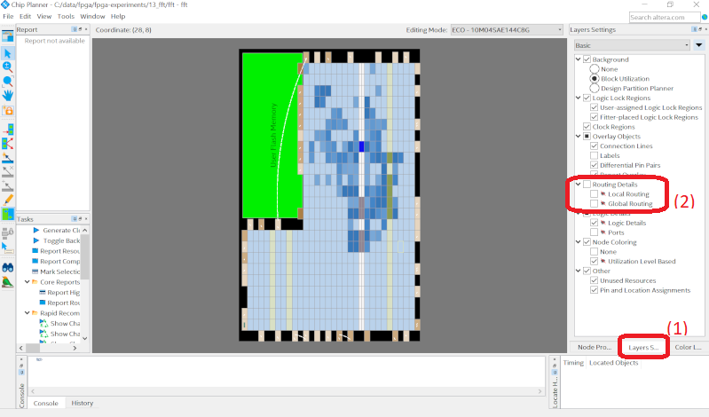
Figure 6. Chip Planner
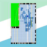
Here we can see the structure of the FPGA chip. Blue are CLB blocks, green are RAM, and brown are DSP. When we zoom in, we will see the internal structure of each block and which parts are used. We can also turn on the connection view. In the left menu, select the Layers tab (1) and select Routing Details (2). The obtained result is presented in Figure 7.
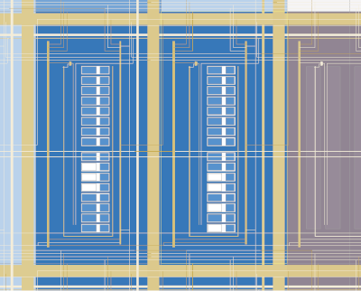
Figure 6. View of connections between blocks
I hope that this short description will encourage you to check for yourself how your projects are implemented. This allows us to better understand the system and use its possibilities.